


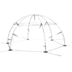

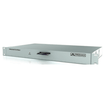


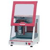


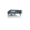


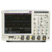


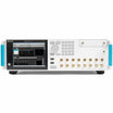
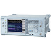


Wentworth S200D Double-sided Probe Station
Use our chat for personal support. Or contact us via +45 31 33 18 19 or salg@GOmeasure.dk
- Simultaneous, double-sided probing of up wafers up to 200 mm (8″)
- Unique caliper arm and probe needle design
- Adjustable wafer size carriers
- Tuneable gram force and speed settings
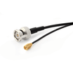
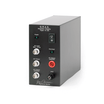
- TTL, Ethernet (10BaseT), RS232 and IEEE 488 control interface
%20%09Unique%20caliper%20arm%20and%20probe%20needle%20design%20%09Adjustable%20wafer%20size%20carriers%20%09Tuneable%20gram%20force%20and%20speed%20settings%20%09TTL,%20Etherne...
)
Discover the possibilities
More information
Description
Wentworth S200D Double-sided Probe Station
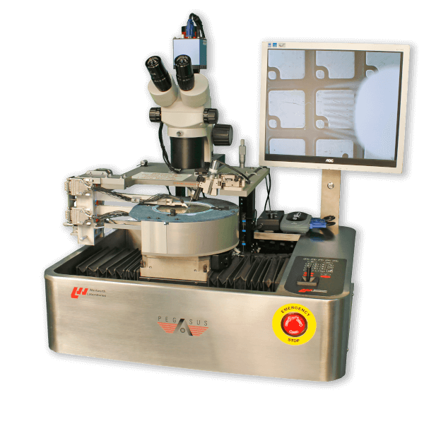
PEGASUS™ S200D
DOUBLE-SIDED PRODUCTION PROBE STATION FOR 200 MM WAFERS
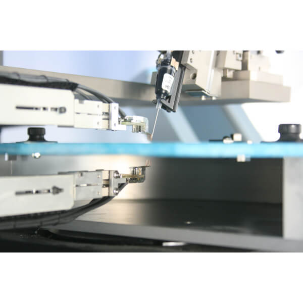
The Pegasus™ S200D semi-automatic production wafer prober is an ideal solution for applications requiring double-sided probing. It is highly recommended for test correlation and engineering design, supporting wafers up to a size of 200 mm (8″).
As a double-sided probing system, the S200D allows the user the flexibility to probe from the top and bottom of the wafer simultaneously.
WIDE RANGE OF APPLICATIONS
- Double-sided testing of discrete power semiconductors, metal-oxide semiconductors and insulated-gate bipolar transistor (IGBT) devices
- Testing of silicon based devices, newer wide-band gap (WBG) materials and compound semiconductors
- Test correlation
DESIGN
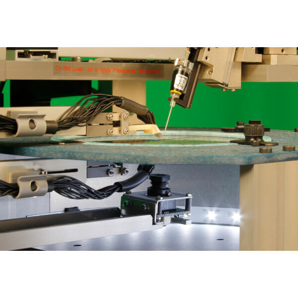
Boasting a similar specification to its single-sided counterpart, the Pegasus™ S200, the S200D enables rapid production probing and provides versatility through its highly configurable platform.
The articulated ‘parallelogram’ motion of its probe tips, ensures that the probes accommodate any variation in the wafer flatness and bow. This achieves even probe marks across the wafer. It also means that probe gram force remains consistent, thus maintaining even contact pressure for accurate and repeatable measurements.
APPLICATIONS
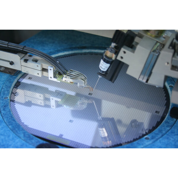
The Pegasus™ S200D wafer prober delivers a robust solution for double-sided testing applications involving discrete power semiconductors, metal-oxide-semiconductor field-effect transistor (MOSFET) and insulated-gate bipolar transistor (IGBT) devices. It is equally suitable for testing silicon-based devices as well as newer wide-band gap (WBG) materials and compound semiconductors such as Gallium Nitride (GaN) and Silicon Carbide (SiC).
The Pegasus™ S200D wafer probe station can eliminate chuck plate influence from test results. It is therefore highly recommended for test correlation or engineering design teams working on the power device types mentioned above.
Documents
Wentworth S200D Double-sided Probe Station
Wentworth S200D DatasheetOptions
Video
Wentworth S200D Double-sided Probe Station
PEGASUS™ S200D
DOUBLE-SIDED PRODUCTION PROBE STATION FOR 200 MM WAFERS
The Pegasus™ S200D semi-automatic production wafer prober is an ideal solution for applications requiring double-sided probing. It is highly recommended for test correlation and engineering design, supporting wafers up to a size of 200 mm (8″).
As a double-sided probing system, the S200D allows the user the flexibility to probe from the top and bottom of the wafer simultaneously.
WIDE RANGE OF APPLICATIONS
- Double-sided testing of discrete power semiconductors, metal-oxide semiconductors and insulated-gate bipolar transistor (IGBT) devices
- Testing of silicon based devices, newer wide-band gap (WBG) materials and compound semiconductors
- Test correlation
DESIGN
Boasting a similar specification to its single-sided counterpart, the Pegasus™ S200, the S200D enables rapid production probing and provides versatility through its highly configurable platform.
The articulated ‘parallelogram’ motion of its probe tips, ensures that the probes accommodate any variation in the wafer flatness and bow. This achieves even probe marks across the wafer. It also means that probe gram force remains consistent, thus maintaining even contact pressure for accurate and repeatable measurements.
APPLICATIONS
The Pegasus™ S200D wafer prober delivers a robust solution for double-sided testing applications involving discrete power semiconductors, metal-oxide-semiconductor field-effect transistor (MOSFET) and insulated-gate bipolar transistor (IGBT) devices. It is equally suitable for testing silicon-based devices as well as newer wide-band gap (WBG) materials and compound semiconductors such as Gallium Nitride (GaN) and Silicon Carbide (SiC).
The Pegasus™ S200D wafer probe station can eliminate chuck plate influence from test results. It is therefore highly recommended for test correlation or engineering design teams working on the power device types mentioned above.